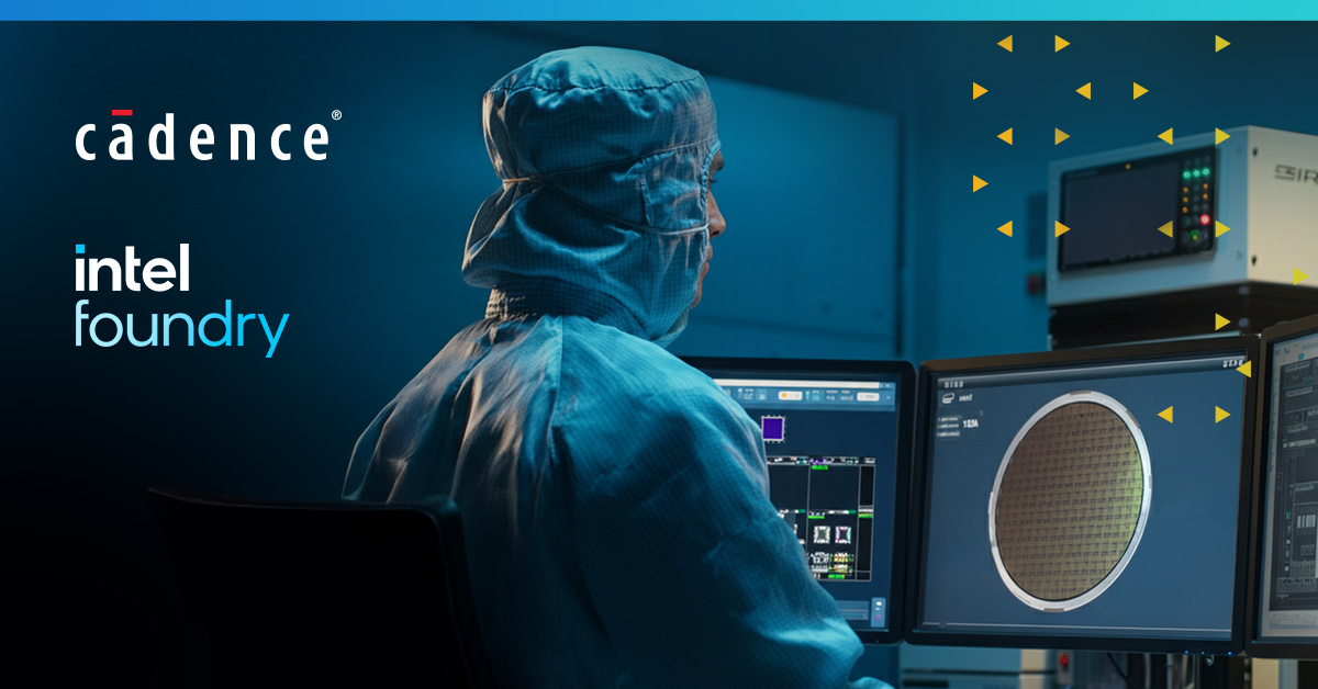
Cadence and Intel Foundry have signed a multi-year agreement to work together on Design Technology Co-Optimization (DTCO) for Intel's 14A process node — giving chip designers one of the tightest EDA-to-fab integrations Intel has offered in years.
The deal combines Cadence's agentic AI-driven EDA tools and Design IP with Intel Foundry's process and packaging expertise. The stated goal is to get tools, flows, and methodologies aligned before the node reaches production readiness, targeting improvements in performance, power, and area (PPA) across both HPC and mobile chip designs.
What the Collaboration Actually Covers
At its core, this is a PDK readiness play. Cadence and Intel will work together to deliver production-ready process design kits (PDKs) for Intel 14A — the documents and libraries chip designers need to actually build layouts that work on a specific process. Without a solid PDK, even a great fab process is effectively inaccessible to outside customers.
Beyond the PDK work, the agreement covers design enablement more broadly: IP readiness, agentic AI-driven design flows, and joint methodology development. Cadence's AI tools will be used to accelerate time-to-market and reduce design risk for customers targeting Intel 14A.
"Advancing our relationship with Intel into a much deeper partnership is a major milestone for both companies," said Anirudh Devgan, president and CEO of Cadence. "This collaboration will leverage the strengths of both companies to empower customers to unlock new levels of performance, power, and efficiency."
Intel Foundry's EVP and GM Naga Chandrasekaran framed it as part of Intel's broader push to deliver on its technology roadmap for customers: "By combining Intel's process and packaging with Cadence's AI-driven design tools, we are enabling deeper co-optimization."
Why This Matters for Intel Foundry
Intel Foundry has been working to attract serious external fabless customers — a business that requires ecosystem trust, not just process capability. A chip company evaluating a new node needs to know their EDA tools work, their IP is certified, and the PDK is production-grade before they'll commit to a tape-out. TSMC has spent decades building exactly this kind of deep ecosystem alignment. This deal signals Intel is taking the same playbook seriously for 14A.
Cadence already has a parallel collaboration with Samsung Foundry on 2nm, announced in May. The company is clearly positioning itself as the go-to EDA partner across all the major foundries competing in the angstrom-era race — which is smart business for Cadence and useful signal for chip designers watching where the ecosystem support is actually landing.
Intel 14A: The Node to Watch
Intel 14A is the next step in Intel's angstrom-era roadmap, following Intel 18A. Intel has positioned 14A as a competitive node for high-performance compute and mobile applications, with backside power delivery and a gate-all-around transistor architecture. Getting the EDA flows right before the PDK is final is exactly the kind of groundwork that separates a node that ships on time from one that slips.
This deal won't change the silicon in your next phone or laptop directly. But for any chip company evaluating Intel Foundry as a manufacturing option, Cadence's involvement de-risks the decision. Watch for PDK readiness milestone announcements as the real measure of progress here.